Welcome to Semi Design
Shape the Future of
Semiconductor
India’s Trusted Platform for VLSI Learning

Services
High Quality Training
Deadline
Project on Time
Support
24x7 Support
Placement
Placement Assistance
ASIC Design & Verification Program
The Job-Oriented ASIC Design & Verification Program is a comprehensive training course tailored to equip participants with the essential skills required in the semiconductor industry. This program focuses on the core principles of Application-Specific Integrated Circuit (ASIC) design and verification, preparing candidates for real-world job opportunities in semiconductor industry.
Design for Testability (DFT) Program
The Design for Testability (DFT) Program is a specialized training course focused on preparing participants for careers in the semiconductor industry's DFT domain. The program covers key concepts such as scan insertion, boundary scan, ATPG (Automatic Test Pattern Generation), BIST (Built-In Self-Test), fault simulation, and test compression techniques.
Peripheral Component Interconnect Program
The PCIe Program is a targeted training course designed to provide in-depth knowledge of the PCIe protocol. Participants will learn the architecture, transaction layers, physical and data link layers, as well as advanced PCIe features like link training, flow control, and error handling. The program includes hands-on experience with industry-standard tools and real-world PCIe projects.
Advanced Verification Program
The Advanced Verification Program in VLSI is a specialized training course aimed at mastering the latest techniques in functional verification for complex VLSI designs. The program covers advanced concepts like SystemVerilog, UVM, assertion-based verification, functional coverage, and constrained-random testing and gain hands-on experience with industry-standard tools.
RISC-V at SoC Level Advance Program
The RISC-V at SoC Level Program is an advanced training course focused on the design and integration of RISC-V processors at the System-on-Chip (SoC) level. This program covers RISC-V architecture, instruction sets, SoC design flow, processor integration, memory subsystems, and interfacing with peripherals. Participants will also learn about verification and validation strategies for RISC-V-based SoCs.
Summer Internship Projects Program
The Summer Internship Projects Program in Design & Verification is an immersive, project-based training designed for students and fresh graduates who want to gain hands-on experience in VLSI design and verification. This program offers practical exposure to digital design, Verilog/SystemVerilog coding, RTL design, and verification methodologies like UVM.
Start Your Career in VLSI
Join our hands-on, industry-focused training programs
Latest Workshop 2026
15 Days Advance UVM Workshop
The 15-Day UVM Workshop is an intensive, short-term program designed to provide a deep understanding of the Universal Verification Methodology (UVM). This workshop covers essential topics such as testbench architecture, object-oriented programming in SystemVerilog, sequences, drivers, monitors, scoreboards, and coverage-driven verification.
RTL & Physical Design Workshop
The RTL & Physical Design Workshop is a comprehensive program that provides hands-on training in both Register Transfer Level (RTL) design and Physical Design for VLSI circuits. The workshop covers RTL coding in Verilog, synthesis, timing analysis, floorplanning, placement, routing, and power optimization techniques. Learn the complete design flow from RTL to GDSII.
Assertion & Coverage Workshop
The Assertion & Coverage Workshop offers practical workshop on using assertions and coverage techniques for VLSI advanced verification. Learn to write SystemVerilog assertions, implement functional coverage, and analyze coverage reports through hands-on projects. Enhance your verification skills and ensure design correctness with industry-standard methodologies.
Why Semiconductor Industry?

High demand
Semiconductors are used in almost all electronic devices, from smartphones and computers to cars and airplanes. The demand for semiconductor technology is rapidly growing, creating numerous job opportunities.

Lucrative salaries
The high demand for semiconductor professionals has led to high salaries, with many positions offering competitive pay and benefits. The semiconductor industry choice for individuals seeking a career with a high earning .

Wide range of roles
The semiconductor industry offers a diverse range of roles, from design and fabrication to testing and quality control. This allows professionals to find the role that best fits their skills and interests.

Career growth
The semiconductor industry provides numerous opportunities for career growth and advancement, with many professionals being promoted to leadership positions within the industry
Overall, a career in the semiconductor industry can be highly rewarding, both personally and professionally. With the increasing demand for semiconductor technology, now is an excellent time to pursue training and explore the opportunities available in this exciting field.
Your Gateway to the Core VLSI Industry
Semi Design is a specialized VLSI training and internship platform dedicated to bridging the gap between academic knowledge and semiconductor industry demands. We provide high-quality, hands-on training programs in RTL Design, Verification (SystemVerilog, UVM), DFT, STA, Physical Design, and more.
Are you Made for VLSI Domain?
Test Your Skills In VLSI Domain
Verilog HDL
SystemVerilog
Digital Design
CMOS Design
Advance Digital Logic Design
focuses on the design, analysis, and optimization of complex digital circuits and systems, including combinational and sequential logic, FSMs, and programmable devices. It prepares learners to tackle modern computing challenges by developing efficient, high-performance digital systems.
Semiconductor Theory & CMOS
Explores the fundamental principles of semiconductor physics and the operation of CMOS technology. It covers the behavior of semiconductor materials, the design and fabrication of CMOS transistors. This knowledge is essential for understanding and designing modern electronic devices and integrated circuits.
Digital IC Design with Verilog HDL
is a hardware description language used for modeling, simulating, and designing digital circuits and systems. It provides a means to describe both the behavior and structure of digital hardware, allowing for efficient design and verification. Verilog supports synthesis and is widely used for developing FPGAs, ASICs, and other digital devices.
Verification with SystemVerilog HVL
is an extension of Verilog, combining hardware description and verification capabilities for designing complex digital systems. It enhances modeling efficiency, supports advanced verification features like assertions and testbenches, and is widely used for designing and verifying FPGAs, ASICs, and other digital hardware.
Universal Verification Methodology UVM
is a standardized framework for verifying complex digital designs in SystemVerilog. It provides reusable, scalable verification components and advanced methodologies like constrained random testing, functional coverage, and assertions, streamlining the process of verifying ASICs, FPGAs, and other digital systems.
IC Layout Design
in VLSI involves transforming a circuit's logical design into a physical layout, preparing it for fabrication. It includes key steps like floor-planning, placement, routing, and timing optimization, ensuring efficient performance, area utilization, and manufacturability of semiconductor chips.
for layout design we need to know transistor level also .
Static Time Analysis
is a method used to verify the timing performance of a digital circuit without requiring simulation, checking for timing violations like setup, hold time, and clock skew. It ensures that the design meets speed and timing constraints, guaranteeing reliable operation under all process, voltage, and temperature (PVT) conditions.
Design for Testability
involves features into a circuit design that facilitate easier and more effective testing during manufacturing, improving fault detection through techniques like scan chains and boundary scan. It ensures high-quality and reliable semiconductor products by enabling comprehensive testing, fault diagnosis, and enhanced coverage of potential defects.
Smart Strategies To Get In VLSI industry
- Master core concepts in Digital Electronics, CMOS, Verilog, SystemVerilog, and UVM.
- Work on real projects to demonstrate hands-on design and verification skills.
- Build a strong resume with keywords aligned to job roles (e.g., RTL Design, DV, DFT).
- Take specialised training or internships from reputed institutes (like Semi Design).
- Practice mock interviews and technical quizzes regularly to boost confidence.
- Create a GitHub portfolio showcasing your code, projects, and documentation.
- Stay updated on industry trends, tools (like Synopsys, Cadence), and EDA workflows.
- Network with professionals via LinkedIn, webinars, or VLSI-focused forums.
- Target fresher hiring drives and off-campus openings proactively.
- Be consistent with your efforts, learning pace, and interview preparation.
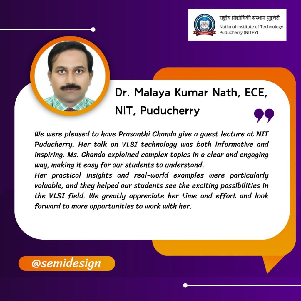
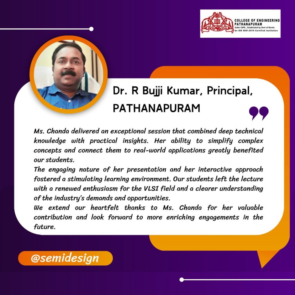
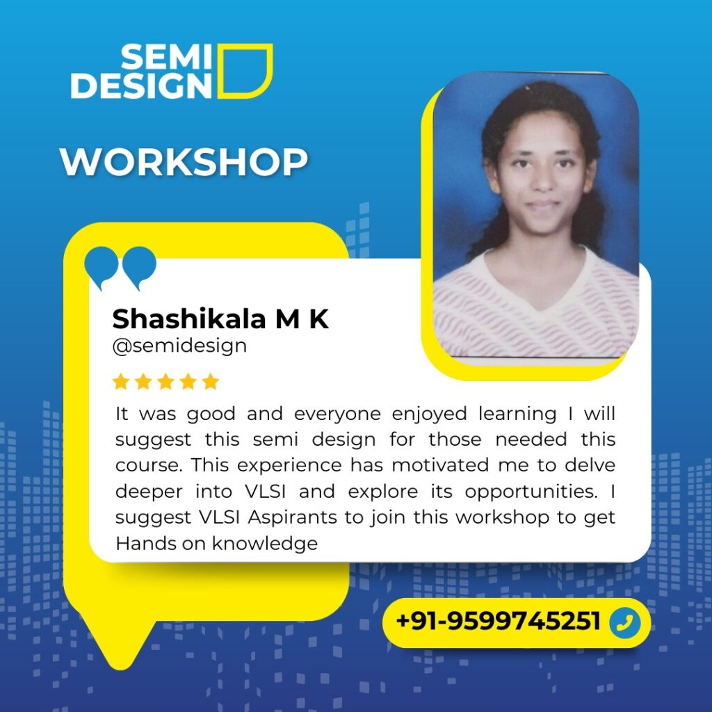
Testimonials from Leading Institutes


The Secret of Success
The secret of success lies in perseverance and continuous learning, turning challenges into opportunities. With clear goals and consistent effort, growth becomes inevitable.
Choose Your Interest
- Know yourself properly
- Always Challenge Yourself
- Make friends with same interests
Be Consistent
- Believe in Continuity
- Be busy for your interest
- Don’t Waste Your Time.
Set Target
- Make a goal
- Be focused
- Hit the Goal
Believing in Yourself
- Self-trust
- Be positive in every situation
- Don’t Fear of Change


